Etching a Copper PCB
How to etch a circuit board
OR
From schematic to copper board, getting it done.
(from July 2006)
I have previously used a milling machine to mill a PCB.
Then I read about easily etching PCB's. This method uses a laser printer to print the circuit pattern onto glossy ink-jet photo paper. The circuit pattern is then ironed onto the copper board from the photo paper. The pattern is then etched into the PCB using hydrochloric acid and hydrogen peroxide. The toner-pattern is then wiped off using acetone.
I tried this method on the 6th of July 2006, and it worked spectacularly: make a near-perfect PCB in about 25 minutes.
This page describes the method, and how to etch your own PCB's.
List of Materials for Laser-Printer PCB Etching
Black and White HP Laser Printer (eg. LasetJet 1020, LaserJet 6P)
Staples Glossy Photo Paper, Item # 471861, Bar Code # 1803 02856
Copper PCB (6"x6", 1/16" thick double sided copper-plated PCB from ABRA electronics.)
Hydrochloric Acid (Hardware store, also known as Muriatic Acid)
Hydrogen Peroxide (Pharmacy, as a disinfectant)
Acetone (nail-polish remover)
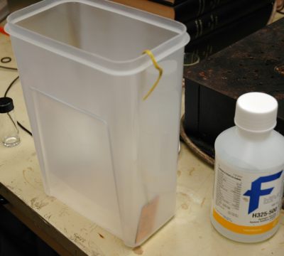
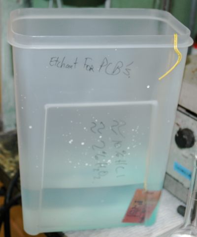
Plastic Container (for the etchant solution, never use it for anything else afterwards)
Permanent Marker (both for labeling the etchant container and for touching up boards)
Iron (as in clothes iron)
Tea-Towel
Piece of Wood
Fine toothed hacksaw blade
Fine-grit sandpaper (600 grit or finer, for wet sanding)
Fishing wire, or metal wire with plastic coating
Drill with fine tip bit (for drilling the via's afterward)
Methodology
First, use a program such as KiCAD or Eagle PCB to design and generate a circuit board layout. KiCAD is free and open source software. Eagle used to have a free version for hobby and students. You should export the top and bottom board layers with all the desired traces to two separate image files. The images below are examples of this. Make sure you output the images at a high resolution (such as 600DPI). KiCAD isn't simple, but it's worth learning, as it will save you from a lot of design difficulties.
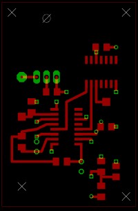
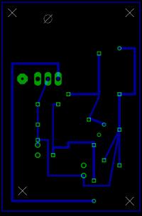
Now use an image editing program such as GIMP or photoshop to turn the images into black and white images, such that the circuit patterns are in black, and the background is white. The top layer should be designed so that the pattern will print onto the paper in reverse. This is because the pattern will be affixed onto the copper, and will be placed face-down. Once the pattern is affixed, the paper backing will be ripped off. So the final circuit will actually look as if you are looking through the back side of the paper.
The bottom side should already be reversed.
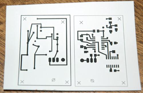
Once you have the black and white images, copy them into a single image document, side by side. Print them onto the Staples glossy inkjet photo paper, such that the toner is printed onto the shiny side of the paper. Here you must use a laser printer. I have used two HP laser printers- a laserjet 1020, and a laserjet 6P. Both printers worked well, and neither seems to have been damaged by printing onto the inkjet paper. Other laser printers may print at a higher temperature, and might be damaged by the glossy paper layer sticking to the rollers in the printer.
Once you have the printed toner-patterns, cut them out carefully, so that you can align two edges onto two edges of the PCB.
Clean the PCB in three steps: use a piece of fine sandpaper (such as 600 grit), use a sandpaper that can be wetted, and make sure to sand while the paper is wet. Next, wash it with soap and water, then dry it. Finally wipe it down with acetone. (Clean both sides of the PCB)
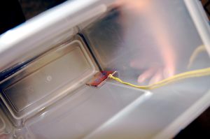
Now set the PCB on top of a dish-cloth, on top of a piece of wood. You will be heating the PCB with a clothes-iron, such that the toner will melt off the paper, and stick onto the copper of the PCB.
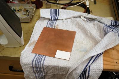
With the iron at maximum heat, pre-heat the copper board by sitting the iron on it for a minute or two. Now position the top pattern onto the first corner of the board. Make sure to line up the sides correctly. The laser-printed photo-paper will stick on, as if you were applying a sticker, not a piece of photo-paper. Make sure you don't push the paper around after it sticks, or the pattern will be blurred.
Now take the iron and place it on the back of the paper. Allow the paper to get hot. You should probably also push down on it, though I didn't apply much force, and it still worked.
To do the other side, you flip over the (hot) PCB, and apply the second side to the corresponding back-face of the PCB. Again, pre-heat the copper board, then apply the photo-paper. Heat it on with the iron as you did for the first side.
If things don't work out with the toner-transfer, don't worry. You can rub the toner off, and clean the board, and restart from the beginning. So don't worry if it doesn't work out quite right at the beginning.
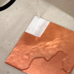
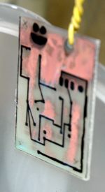
Now that you have the two pieces of printed paper stuck on the copper board, put it in water for a few minutes. I ran mine under cold tap-water. You can try getting water under the edges of the paper, and it seems to get wet faster. The paper is quite thick, but if you let it get wet for a few minutes, the paper becomes fairly transparent. After a while, you can see the pattern through the paper. The paper will unstick from the copper surface, and it won't require much force to pull the paper backing off. There will probably be a thin film of paper left in some of the more detailed areas, and on the backs of the traces. Brush softly with a soft toothbrush, and the paper film will come right off. This should leave a near-perfect circuit pattern left on the copper. If there are missing bits, you can touch it up with a permanent marker, though the marker won't be as nice a mask as the toner.
Again, if you pattern isn't nice, you can clean off the board (acetone), and re-apply a newly-printed pattern.
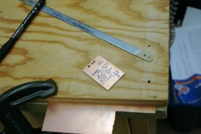
You will probably want to cut the board to shape (I used a fine-tooth hack-saw blade in my hand, with the board c-clamped onto the lab-bench surface). Also helpful is to drill a hole through which to hang the PCB during the etching process.
Now that you have a toner-protected PCB, you need to etch the circuit.

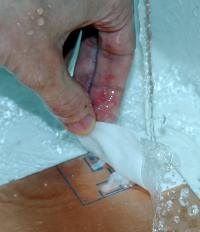
You will make a 10% hydrochloric acid (HCl), 2% hydrogen peroxide (H2O2) solution. I used 40% HCL, and 30% H2O2 stock solutions, so I needed to dilute them more than most people would. I simply added enough water at the bottom of a plastic container to cover the circuit board. Next I added about 1/4 of the volume of HCl, and another 1/15th fo H2O2. Note that I didn't even measure. This is just a solution for eating the copper off the board, it doesn't need to be a detailed and precise solution. Wearing a lab-coat and rubber gloves (think dishwashing gloves) is probably a good idea.
A key concept here is that adding ACIDS to WATER should always be done in that order. Take lots of water, and SLOWLY add the concentrated acid to the water. The water will get hot. Do it slowly. If you add water to the concentrated acid, it will suddenly boil, and splash concentrated acid everywhere. Including on you. Many people have been burned quite badly by acid by adding water to acid, and I really don't recommend you try it.
The acid solution should be clearly marked, and stored in a well-ventilated area away from foods, metals, acids, bases and other things that you don't want to have damaged. To dispose of the solution, you can probably pour it down the drain, along with a lot of water. The key would be to pour it SLOWLY, while leaving the tap flowing at full. Warning: Pouring a concentrated acid solution into your pipes would probably eat through them. Alternately, you could use a base to neutralize the acid, and verify using some pH paper. Keep in mind, this solution can EAT THROUGH METAL, so be careful.
Once you have your etchant (acid solution), you tie the PCB onto a plastic string (fishing wire, or plastic-coated electrical wire) and lower it into the etchant. Within moments, you will see a blueish-green tint appear in the etchant. That's the Copper Chloride folks, you're successfully dissolving the copper off the surface of the board.
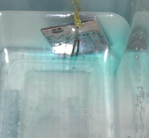
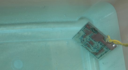
Let it go for a few minutes, while agitating the board every once in a while (to displace bubbles).
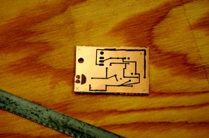
The copper will disappear. It took less than 5 minutes for me, to get to the last of the etching photos. Now pull the board out, and rinse it off thoroughly. (There was concentrated acid on it, so make sure you rinse for a few minutes)
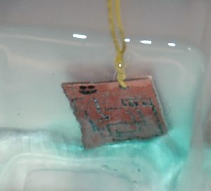
Now you can take the acetone and wipe the traces off the board.
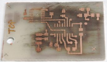
When I did this, some of the toner (or perhaps the pen-ink) smudged onto the silicon board, and I couldn't get it off afterwards. It doesn't affect the circuit, but it's ugly. You might consider using an acetone bath, and wiggling the board in the bath until it's clean. Note that your plastic string will likely be dissolved by the acetone. Don't get acetone all over yourself: it's bad for you.
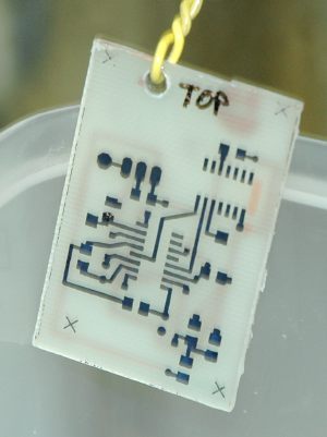
That's it! You now have a cleanly etched PCB. I think even the finest surface mount circuits can be printed like this. I'd estimate 20 minutes to print and etch a circuit, so this is REALLY fast.
The only thing left to do is drill the via-holes. I'd suggest doing that with a Dremel and dremel-drill-press, unless you happen to have a CNC milling machine.
Enjoy!